The internet is full of info about how to make printed circuit boards, just Google it, look at Make Blog or go to Instructables. So I won’t go into detail in these notes but, here are a few of my tips that I that I think are lacking elsewhere. Even though prices to get PCBs commercial made have been coming down a lot, sometimes you want a one off, or a prototype to test a design.

The method that I have been using with success incorporates using presensitized cooper clad boards. Some say that they are too expensive, but for most of my projects I only need a few square inches at a time, so the board is only a few cents per project. Ink Jet paper transfer methods do work, but I have found it a lot of trouble and in my experiences this method was only good for circuits made with large components. The nice thing about presensitized boards is that the resolution of your lines is mostly limited by how well your laser printer prints onto transparency films and not the cooper board. For example in the title of this page the traces go down to 8 mils leading to the QFN28.
To use the EPS files from the from the link below you should first print them on transparency slides (the type that are used for overheads, available from Staples). You will need a Postscript Laser printer to do so. I have tried to open the EPS files in Adobe Acrobat or Preview on the Macintosh then printing, but the scaling is off a little. On the Mac I just drag the file onto the printer in the Printer Setup Utility and it prints directly to the printer. The design is reversed so that the printed side (with the laser toner) will be placed next to the PCB. Sometimes you may have to print two copies and lay them on top of each other if a single print is not dark enough.

After the positive artwork is ready, follow the directions that come with presensitized cooper boards. Some experimenting may have to be done to adjust and exposure and developing time. I like to go a little bit longer on the exposure, it makes developing the boards a little easier. When developing the boards it is very important that all of the resist be off, of the areas that you want etched. Even a very thin film will possibly ruin your board because you will have to etch it longer and then loose the fine details. The technique that I use is, to develop the board, then put it under running water to rinse. When I take it out of the rinse, if after ten seconds or so, the water beads differently between the etched parts and the copper parts then I know it is done, if not I develop a bit longer.
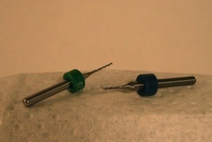
Drilling holes in PCBs is miserable, especially with the bits that you get at some hobby and or electronic shops (the ones that look like very small regular bits). What I use are the 1/8 inch carbide bits. I still don’t like drilling holes but the process is a bit more pleasant with these bits. I don’t try to drill by hand any longer (too many broken bits). Put one of these carbide bits in you drill press, put on you safety glasses, set the drill press to it’s maximum speed, turn on the vacuum and let’r rip. A good bit will be like a hot knife though butter, but don’t be fooled these bits are fragile, I am yet to not brake one simply by dropping it on the floor.
Now your board is ready for soldering! If you are new at this there are many sites with soldering tutorials.


Copyright SpikenzieLabs 2019
