Through-Hole soldering is fast, fun and easy. The parts you populate your PCB’s with are the very same ones you can pull from your breadboard once your project is finished, and you are ready to make a permanent version.
What if the components end up taking up too much space for the size of your product? What if the components you need to use are only available as SMD parts, and you were using break-out-boards for them while prototyping?
In this quick tutorial, I will show you how easy it is to make a ‘Mylar’ stencil, that you can use for short runs. It will cleanly and easily apply solder paste to a PCB with surface mount parts (SMT). Mylar isn’t the best material for making a solder paste stencil, but it is really cheap and you can find it almost everywhere, and heck, it does an OK job.
Here is a quick demo video that shows what it looks like when you are reflowing solder paste. As soon as we received our first few boards for our Solder : Time II watch, we wanted to figure out a quick way to paste up a PCB. Our steel stencil took a few days to arrive, we wanted to try out these new PCBs right away.
We used a ‘Mylar’ stencil to put solder paste on this board. Notice how the components ‘self-center’ themselves. The surface tension of the liquified solder paste automatically centers each component, provided they are more or less properly aligned.
We will be using EagleCAD and Illustrator with a 45 Watt Epilog Laser Cutter. The techniques should be the similar if you are using other software. If you have access to a different laser cutter at your local hacker space, tech-shop etc, you may have to fiddle with the power setting we suggest to get them right for your machine.
Step One: Creating an .eps from EagleCAD
")
Click On Cam (Film Strips Highlighted in Photo)
Click on CAM (Highlighted in photo)
This will bring you to the next screen (below) and Step Two.
Step Two: Outputting from EagleCAD
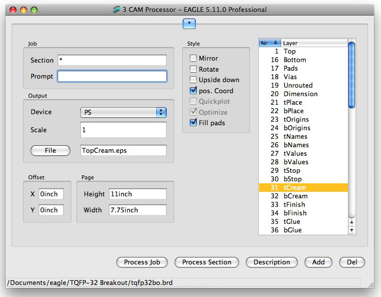
With this window up in EagleCAD, you need to do the following.
OutPut:
A. Device [Set to PS]
B. Scale [Make sure that it is 1]
C. File [Type the name of your file, and end it with “.eps”]
Layers:
Be sure that only the layer 31 tCream is selected. (Deselect all of the other layers)
Do it:
Click the button [Process Job].
In your project file directory of your Eagle schematic and board files you will find the .eps file that EagleCAD created, and this is the file you will be opening in Illustrator.
Step Three: Adjustments in your Illustration Software

Open the saved “.eps” file in Illustrator. We have found that stencils for components that have really fine pitched pads, need a little bit of tweaking before sending the file to the laser cutter. It’s not that there is a problem with the file but rather the way the laser cutter burns through the mylar. Leaving the edges “microscopically” burnt so some resolution is lost. This can be a problem with fine pitch parts.
Our experience has been that decreasing the width of each pad by 20% makes the spacing between the laser created holes larger, leaving a slightly thicker piece of Mylar between pads, increasing the durability of the stencil, as well as limiting the amount of solder paste that gets applied. Solder paste can be used very sparingly, while still having more than enough to make a solid solder joint. Keep in mind that too much solder paste can turn into a ‘jumper’ situation after the board has been reflowed.
Ungroup the pads, select one of them, and make a copy at 80% width. Repeat. The new pads will be 20% less wide than the original. In experiments that we have done, these thinner pads make the super thin strip of mylar between pads thicker and still allows plenty of solder paste through to make a great solder joint.

Here, in our example the thinner pads are shown in grey, over the original sized black pads. We then erase the original black pads, leaving only the grey ones.
Components on your PCB like resistors, caps, SOIC parts and other ICs that have thicker, and less fine pitch legs don’t necessarily need this same treatment. There is a sweet-spot for the thickness of laser beam kerf, and really fine pitched components. You can get away with a great deal more, when dealing with larger & wider spaced pads.
Step Four : Preparing for Laser Etching
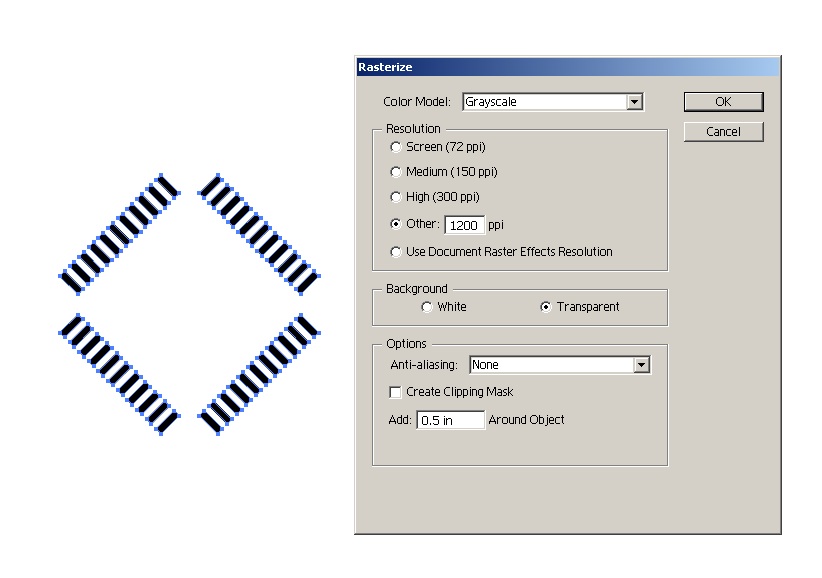
When you’re using a Laser Cutter, there are two ways to make holes in things. You can vector cut, and etch. If the medium you want to cut holes in is thin enough, you can get a much more detailed & precise hole by etching right through, rather than cutting holes in a ‘band saw’ type of way.
Select all of the pads in your illustration, open the Rasterize menu, and convert your vector art into a rasterized image at 1200 ppi.
Draw a box around your PCB. The larger the better, you are going to want a large surface area around your components to accomodate the edges of your squeegee. The larger surface area also gives a larger area for contact with the tape that is holding your stencil solid in place.

The settings that we have uncovered as perfect for our 45 Watt Epilog Helix is as above.
1200 DPI, 40% Speed, 25% Power.
Tape your mylar sheet to a backing sheet of regular paper. And hold everything in place inside the Laser machine with masking tape. If you have a strong enough air exhaust, it can flutter paper sheets, if they aren’t secured.
Step Five : Pressing GO

Here the rastering mode of the laser, is actually printing all the way through the the Mylar sheet, making really precise holes that will act as a stencil to allow just enough solder paste through onto the PCB.

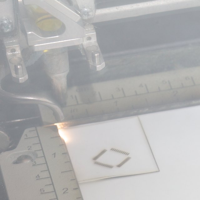
For the purpose of this tutorial, I went with a small cutout. If I was using this stencil for an acutal PCB, it would be about 5x larger.
Notice the amount of remaining Mylar between the pad holes. Any less, and the squeegee would wear it out prematurely.
Step Six : Test Stenciling Solder Paste

Macro closeup of the stencil aligned onto the PCB. We use Kapton tape to hold the stencil into a jig made up of same thickness scrap PCBs. The more time you spend precisely aligning your stencil, and taping it down firmly, the fewer boards you will need to re-do.
We hope you’ve found this tutorial informative. Surely if you’ve done this on your own, you may have other tips and techniques that we have not included. We would love to hear about successes and failures of your own experimentation. Please add them in the comments!
For small jobs, mylar sheets are good, but the Mylar wears out, gets solder paste around to the backside, and needs to be replaced frequently.
After you have tested your PCBs, with this method, and have a few functional units work to your liking, you may want to think about getting a stainless steel stencil made. There is a big difference between the mylar and stainless steel. The $0.50 worth of Mylar sheet helps you find out ahead of time that the $100 + you’re going to spend on the steel stencil is not a waste of money.
Thanks for the page. I have some boards coming from seeedstudio soon. I’ll try the technique.
In the past, I have had some success in cutting the Polyimide tape directly.
I am excited to try this process with the tape adhered to some paper product. I’ll try to post results here.
Laser cutting machines are uses a laser to cut metal sheets. It is typically used in industrial areas and it is also used in small business.
Great post! Thank you for sharing this informative blog. Keep us inform like this.
Really a Very helpful DIY for Solder Pasting. I am also from electronics field and always looking for the new ways of PCB soldering. Thanks for sharing the useful information with us!